English




What Are The Functions of Indium Phosphide (InP) in Optical Modules?
The true core strength and the industry's biggest bottleneck—Indium Phosphide (InP) —is the only core substrate material for high-speed optical modules, EML lasers, detectors, and optical chips . China holds more than 70% of the world's refined indium production capacity and has long included indium phosphide in its export control list. Coupled with the continuous explosion of AI computing power, the more overseas countries restrict the import of complete machines, the more prominent the self-control and scarcity of upstream InP materials and optical chips become, further exacerbating the tight supply and demand situation of global high-speed optical modules!
I. Four Core Components Support The Entire Optical Module
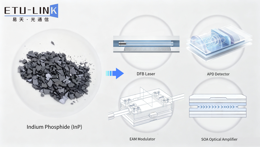
1. InP-based DFB laser: The only reliable light source
No matter how advanced the silicon photonics solution is, it cannot create lasers for the communication band; an external InP DFB light source is required .
InP is a direct bandgap semiconductor. Electron-hole recombination can directly emit light. Its wavelength falls precisely within the ultra-low loss window of 1310/1550nm optical fiber, providing stable, narrow-linewidth, and low-noise single-mode laser output. It is the basic light source for all high-speed optical modules.
2. InP EAM modulator: High-speed optical switch (EML core)
High-end long-distance modules of 800G and above are equipped with EML chips as standard, and EML = DFB laser + InP electro-absorption modulator (EAM) monolithically integrated.
Relying on the QCSE quantum Stark effect, the voltage rapidly switches the light on and off, achieving ultra-high-speed electro-optical conversion with a bandwidth exceeding 50GHz and excellent signal quality, representing the performance ceiling for high-speed, long-distance transmission.
3. InP PD/APD detector: Core components for optical signal reception
Transmission relies on InP, and reception also depends on InP.
Silicon materials have almost no response to 1550nm light, while InP-based detectors can efficiently convert optical signals into electrical signals, and APDs can also avalanche amplify weak signals, making them perfectly suited for high-speed, long-distance receiving scenarios.
4. InP SOA optical amplifier: Lossless optical power compensation
It directly amplifies optical signals without photoelectric conversion, compensating for fiber optic transmission loss, adapting to long-distance transmission and high-end PIC integration scenarios, and significantly improving optical path stability.
II. The Transition from 400G to 3.2T: A Surge in InP Demand
The amount of InP used varies drastically depending on the optical module's speed, and the production capacity bottleneck becomes progressively larger:
(1)400G Optical Module: Only a small number of long-distance models use DFB chips; low InP consumption; ample supply and demand.
(2)800G Optical Module: Fully equipped with EML chips, significantly increased InP substrate and epitaxial growth, revealing a capacity gap.
(3)1.6T/3.2T Optical Module: The number of InP chips per module doubles, and substrate and epitaxial capacity become the biggest bottlenecks in the industry.
Even the currently popular "silicon photonics + thin-film lithium niobate" solution only solves the modulation problem, not the light emission problem, and still relies 100% on InP light sources.
III. Why Is InP Constantly in Short Supply, with Orders Backlogged Through 2027?
1.Extremely stringent epitaxial precision: Nanoscale multilayer quantum well growth with an error not exceeding 1nm and an extremely low yield.
2.Zero tolerance for grating etching: Nanoscale periodic structure, a single error renders the entire wafer unusable.
3.Scarcity of substrate supply: InP single crystals are difficult to grow and are brittle, requiring only 2/3/4-inch small wafers, which are far more expensive than 12-inch silicon wafers.
4.Dedicated production line monopoly: Cannot use general-purpose CMOS production lines; must use dedicated III-V production lines. Very few players worldwide can mass-produce these products.
IV. Core Conclusion: InP Is Irreplaceable and Will Remain in Short Supply in the Long Term
Many people mistakenly believe that silicon photonics and lithium niobate will replace InP, which is essentially a misconception:
Silicon Photonics: It does not emit light and can only be used for optical path integration.
Thin-Film Lithium Niobate: only enhances high-speed modulation, still has no light-emitting capability.
InP: The only all-around material that simultaneously achieves light emission, modulation, detection, and amplification.
As 1.6T/3.2T optical modules gradually ramp up production, the capacity bottlenecks of InP substrates, epitaxy, and EML chips will persist throughout the entire AI computing power construction cycle, making it the most certain high-growth track in the upstream of optical modules.
That concludes this article. Welcome to follow ETU-Link Technology Co., Ltd.. We will continue to share cutting-edge technologies, industry chain dynamics, and industry science popularization in optical communications, and provide an in-depth understanding of the core underlying industry logic of computing power optical networks.
For inquiries about our products or pricelist, please leave your information with us and we will be in touch with in 24 hours.


 13th Floor, Building 6, Honghualing Base, Nanshan Intelligent Manufacturing Base, Liuxian Avenue, Taoyuan Street, Xili, Nanshan District, Shenzhen, China
© Copyright: 2026 ETU-Link Technology CO ., LTD All Rights Reserved.

IPv6 network supported
Friendly Links:
易天官网