English


What are the packaging processes of optical devices in optical modules?
It is believed that everyone should be very familiar with the packaging of optical modules after reading the previous articles of ETU-LINK. So how much do you know about the packaging of optical components in optical modules? In this article, ETU-LINK will take you to understand the packaging process of optical devices.
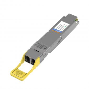
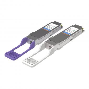
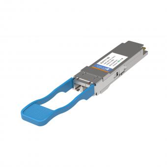
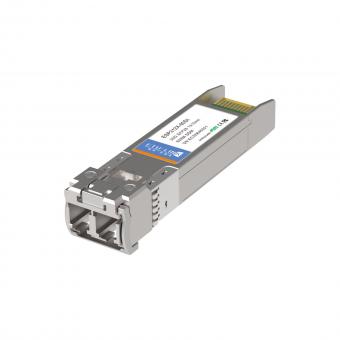
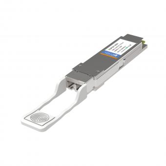
At present, the common optical device packages include Box, COB, TO-CAN, and butterfly packages. Among them, the Box package is commonly used in carrier-grade optical modules. It is a rectangular metal shell with a gold-plated surface, which can be divided into two parts: base and cover.And the chip and lens are attached to the base.
COB package is the abbreviation of chip on board, which belongs to butterfly package and is widely used in Ethernet data center optical transceivers. COB refers to directly attaching bare die chips such as TIA and LDD to the copper foil of the PCB, then gold wire bonding for electrical connection, and finally adding a cover or dispensing protection on the top of the chip.
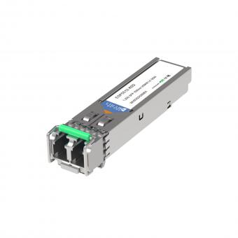
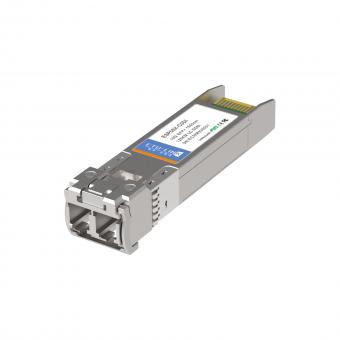
TO CAN package is commonly used in SFP small package optical modules, the full name is Transistor Outline, which is a transistor package. Divided according to the diameter of the base, the common ones are TO56, TO42, TO52, TO38, and more are the size specifications customized by the manufacturer.
Butterfly encapsulation shell usually a cuboid in appearance, structure and realization of function is usually complicated, can be a built-in refrigerator, heat sink, ceramic base, chips, thermistors, backlight control, and can support all of the above parts of bonding wire. And the shell area is large, the heat dissipation is good, and it can be used for various speeds and 80km long-distance transmission.
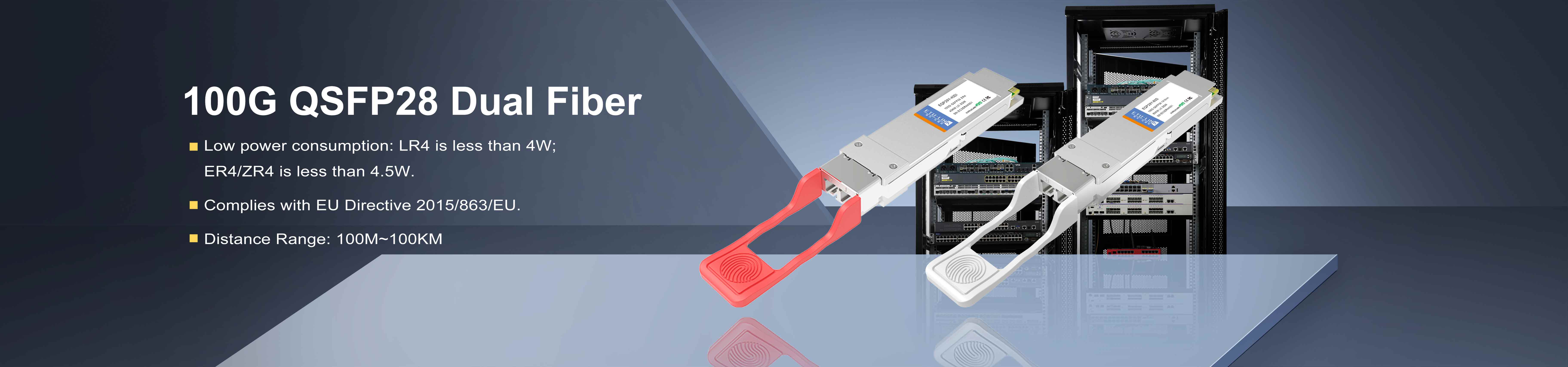
Optical modules with rates of 25G and below mostly use single-channel TO CAN package or butterfly package, with standard process and automation equipment, and low technical barriers. However, for high-speed optical modules with a speed of 40G or higher, it is mainly implemented through multiple channels in parallel due to the laser rate limit. For example, 40G is implemented by 4*10G, while 100G is implemented by 4*25G. The packaging of high-speed optical modules puts forward higher requirements for parallel optical design, high-speed electromagnetic interference, volume reduction, and heat dissipation under increased power consumption. As the rate of optical modules is getting higher and higher, the baud rate of a single channel is already facing a bottleneck. In the future, to 400G and 800G, parallel optical design will become more and more important.
For inquiries about our products or pricelist, please leave your information with us and we will be in touch with in 24 hours.


 Factory: Right Side Of 3rd Floor, No. 102 Building, Longguan Expressway, Dalang Street, Longhua District, Shenzhen
Office: Floor 4, Building 4, Nanshan Yungu Phase ll, Taoyuan Community, XiliStreet,Nanshan District, Shenzhen
© Copyright: 2026 ETU-Link Technology CO ., LTD All Rights Reserved.

IPv6 network supported
Friendly Links:
易天官网