English


The Evolution of Optical Module Packaging From Bulky to Small
In scenarios like 5G live streaming, AI computing, and cloud storage, data flows at a rate of several terabytes per second. The unsung heroes behind this "data voyage" are optical modules—the "optical communication translators" that precisely convert electrical and optical signals.
The packaging technology of optical modules is the "genetic code" that determines their performance, cost, and applicable scenarios. From the "giant" era of GBIC in 1995 to the "nanoscale" integration of QSFP-DD today, what technological leaps has optical module packaging experienced?
This article will use plain language to take you through the evolution of optical module packaging, and will also include a detailed table of package types and matching rates.
Ⅰ. First Generation Packaging (1995-2000): Initial Exploration of Standardization, From "Handicraft Workshop" to "Industrial Assembly Line"
Background: In the mid-1990s, fiber-optic communications entered a period of rapid development, but the optical module market was experiencing a period of rapid growth. Different manufacturers' module sizes, interfaces, and pinouts varied, resulting in interoperability issues. In 1995, operators and equipment manufacturers jointly established the Multi-Source Agreement (MSA) to promote optical module standardization, which led to the emergence of the first generation of packaging technology.
Representative package:
1. 1×9 Package:
Features: Welding design, speed not higher than 1 Gigabit, mostly uses SC interface (large square interface).
Application: Early Ethernet switches and routers have been eliminated due to their large size and poor compatibility.
Case: When an enterprise upgraded its old computer room, it was discovered that a large number of 1×9 modules could not adapt to the new equipment and ultimately had to be replaced with SFP modules.
2. GBIC (Gigabit Interface Converter):
Features: Gigabit speed, large size (about half the size of a palm), 20-pin connection, and hot-swappable.
Application: Mainstream data center and metropolitan area network core equipment around 2000.
Pain point: Due to its large size, a single switch can only accommodate eight GBIC modules, limiting port density.
Technical significance: The first-generation packaging solved the "compatibility" problem of optical modules and laid the foundation for subsequent technological iterations .
Ⅱ. Second Generation Packaging (2000-2018): Miniaturization Revolution, From "Big Mac" to "Mini Elf"
Background: As data centers expand, higher requirements are placed on the volume and density of optical modules. Second-generation packaging focuses on miniaturization, significantly reducing module size through optimized design.
Representative Package:
1. SFP (Small Form-factor Pluggable):
Features: The optical port area is only about 1/3 of GBIC , supports Gigabit speed, adopts LC interface (miniaturized interface), and supports hot plugging.
Application: It became mainstream after 2000 and is widely used in data centers, enterprise networks, and 5G base stations.
Case: A cloud computing company increased the port density of a single switch by three times and saved 60 % of cabinet space by replacing GBIC with SFP.
Features: The speed is increased to 10G, the volume is the same as SFP, the internal CDR module (clock data recovery) is eliminated, and the power consumption is reduced.
Application: After 2009, it became the core module of 10 Gigabit Ethernet, replacing the early bulky XENPAK/XFP.
Data: SFP+ modules cost 40% less than XFP and consume 30% less power, rapidly dominating the market.
Features: Supports 4-channel transmission, 10G per channel, total rate up to 40G, and the volume is only slightly larger than SFP+.
Application: After 2012, it became the mainstream solution for 40G data centers, replacing large modules such as CFP.
Advantages: Compared with CFP, QSFP+ has a port density that is four times higher and a cost that is 60% lower.
Technical significance: The second-generation packaging solves the "density" and "cost" issues of optical modules through "miniaturization" and "multi-channel" design, promoting the large-scale deployment of data centers and 5G networks.
Ⅲ. Third-generation Packaging (2018 to present): High Speed and Integration, From "Electrical Signals" to "Photonic Chips"
Background: With the rise of high-bandwidth applications such as AI and 8K video, optical module speeds are evolving from 40G to 100G, 400G, and even 800G. Third-generation packaging, centered on high speed and integration, is breaking through traditional packaging bottlenecks through innovations like silicon photonics and co-packaged optics (CPO).
Representative Package:
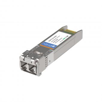
1. QSFP28:
Features: Supports 4-channel 25G transmission, with a total rate of 100G, and the same size as QSFP+.
Application: After 2014, it became the core solution for 100G data centers, replacing large modules such as CFP4.
Data: The power consumption of QSFP28 modules is 50% lower than that of CFP4, and the cost is 40% lower.
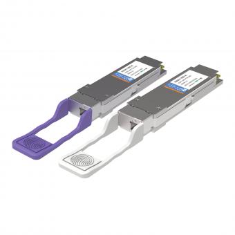
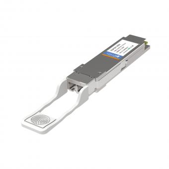
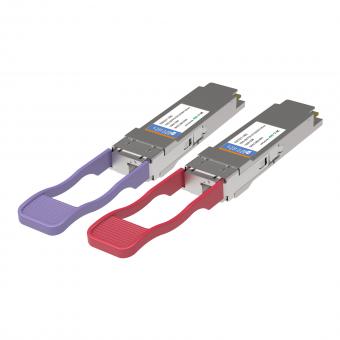
Features: Supports 8-channel 25G/50G transmission, with a total rate of 200G/400G, and the same width as QSFP28.
Application: It will become the mainstream solution for 400G data centers after 2019, supporting high-bandwidth scenarios such as AI clusters and supercomputing centers .
Case: An AI manufacturer increased its internal data center bandwidth by four times and improved large model training efficiency by 30% by deploying QSFP-DD modules.
3. CPO (Co-Packaged Optics):
Features: The optical chip and the switch chip are directly packaged together, eliminating the "electrical signal-optical signal" conversion bottleneck of traditional optical modules.
Application: Pilot projects will begin after 2023 and are expected to become the core solution in the 800G/1.6T era.
Advantages: CPO can reduce power consumption by 50% and latency by 70%, and is the "ultimate form" of future optical communications.
Technical significance: The third-generation packaging solves the "bandwidth" and "energy efficiency" problems of optical modules through "high-speed" and "integrated" design, providing support for high-bandwidth applications such as AI and the metaverse.
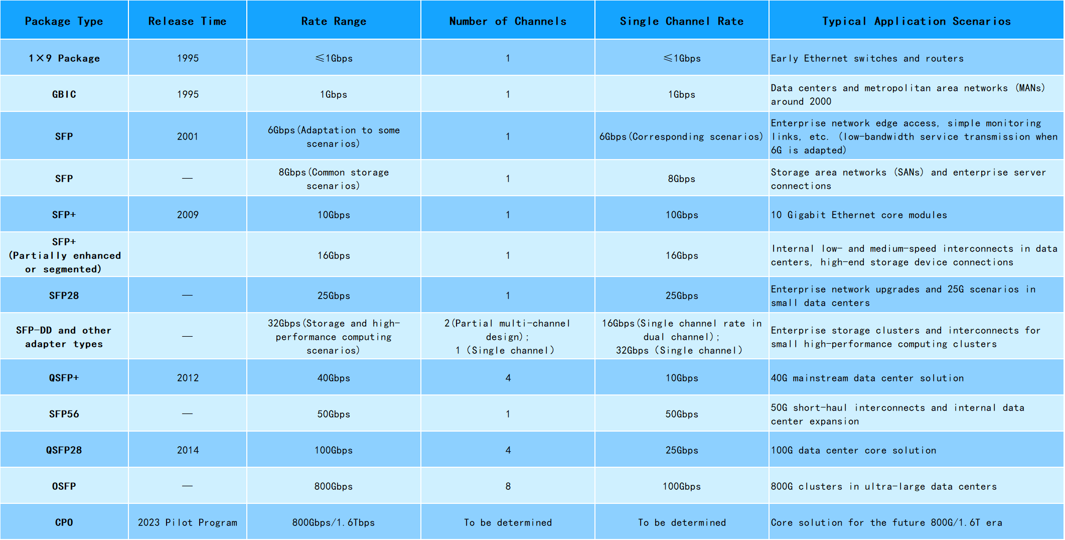
Ⅳ. Optical Module Package Type and Matching Rate Comparison Table
Ⅴ. The Core Logic of Packaging Technology Iteration: The “Impossible Triangle” of Cost, Density, and Performance
Each iteration of optical module packaging represents a balance and breakthrough in the three core indicators of "cost", "density" and "performance":
The first generation: takes "standardization" as the core to solve compatibility problems, but is large in size and low in density.
Second generation: With "miniaturization" as the core, it improves density and reduces costs through optimized design, but the speed is limited by the bottleneck of electrical signal transmission.
The third generation: With "high speed" and "integration" as the core, it breaks through physical limitations through technologies such as silicon photonics and CPO, but the cost is relatively high and needs to be gradually popularized.
Ⅵ. Future Outlook: What is The “Ultimate Form” Of Optical Modules?
With the advent of the 800G/1.6T era, optical module packaging will face two major challenges:
Thermal management: High-speed signals generate a lot of heat, and the heat dissipation problem needs to be solved through technologies such as liquid cooling and 3D packaging.
Cost: New technologies such as CPO are expensive and need to be reduced through large-scale production.
In the future, optical module packaging may evolve in two directions:
Short term: High-speed pluggable modules such as QSFP-DD and OSFP are still the mainstream, meeting the needs of data centers and 5G upgrades.
Long term: After CPO technology matures, optical modules will be deeply integrated with switching chips and become part of the "photonic chip", completely subverting the traditional packaging form.
VII. Conclusion
From "big guy" to "little elf", the evolution of optical module packaging is a history of practicing the "bone shrinking skill" of optical communication technology.
From the "Big Mac" era of GBIC in 1995 to the "nano-level" integration of CPO today, each packaging iteration has promoted a leap in data transmission efficiency.
In the future, with the rise of high-bandwidth applications such as AI and the metaverse, optical module packaging will continue to evolve in the direction of "higher, faster, and stronger", building a more efficient and greener "optical communication highway" for the digital world.
Categories
New Blog
Tags
For inquiries about our products or pricelist, please leave your information with us and we will be in touch with in 24 hours.


 Factory: Right Side Of 3rd Floor, No. 102 Building, Longguan Expressway, Dalang Street, Longhua District, Shenzhen
Office: Floor 4, Building 4, Nanshan Yungu Phase ll, Taoyuan Community, XiliStreet,Nanshan District, Shenzhen
© Copyright: 2026 ETU-Link Technology CO ., LTD All Rights Reserved.

IPv6 network supported
Friendly Links:
易天官网