English


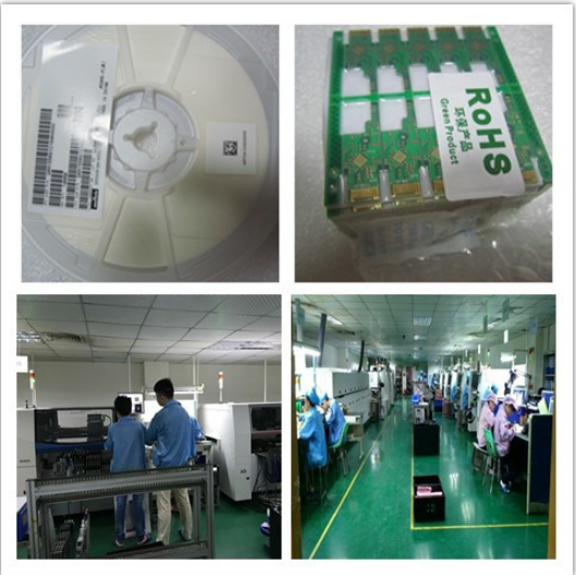
The Production Processing of Optical Transceiver
As a manufacturer, we strictly control the product quality from the marterial. From the project selection, PCB board design, PCB proofing, to the small batch of products, selection of optoelectronic components manufacturers, as well as the procurement and selection of supporting packaging materials and production materials and so on. Each step is strictly according to the industry standards, exceed the requirements of peers to achieve high quality of products. At the beginning of the project selection,our company selects large electronic components / chip suppliers. ETU-Link selects Murata, TDK,Too lure, Yageo electrical components; As the chip, we select the First class agent---Maxim. The design of PCB board wiring is practical and beautiful. For the quality of board, our hardware engineer is very strictly on the gold plating, the thickness gold finger must be over 0.38um. Sample test will be repeated when Proofing and small batch test. Strive to maximize the optimization of PCB programs to ensure the stability and consistency of bulk shipment.
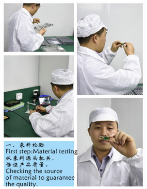
All batch of materiel will be tested.Take the core material Optoelectronic components for example. As below picture:
※ Material testing, come to the first step---Welding. Before welding, the electronic device will be cut. The operation as shown below:
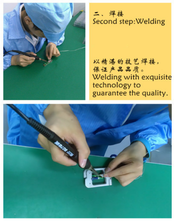
※ Welding should pay attention to: The length of the shear pin should be consistent, these require our workers must be focused and skilled.
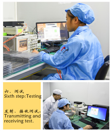
We will conduct the initial test, visual inspection and microscopic examination for the semi finished products.
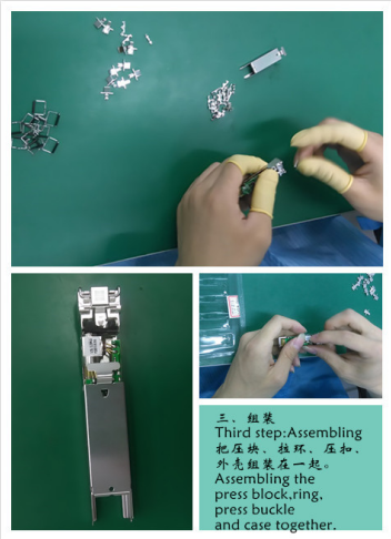
※ Assembling, the operation as shown below:
※ Writing A2 and aging testing, to ensure the stability of the product.
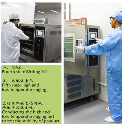
※ High and low temperature aging test, will test the Transmitting optical power, receiving sensitivity and other parameters.
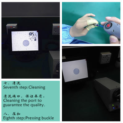
After the above testing,we will clean and lock stamping parts for the good one, pick up the defect product, then returned to repair area for repair and retest.
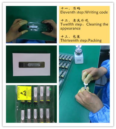
Labeling and packaging, see the following picture:
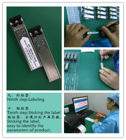
※ Writing A0 information after labeling,then test on the switch and packaging.
Everyone focus on every step during the production process. Because we deeply recognized, quality is the only thing we insist on the road. Each one in ETU-Link Technology Co., Ltd are adhering to the conviction of quality first, service first. Strive to do every detail well to win customers.

Categories
New Blog
Tags
For inquiries about our products or pricelist, please leave your information with us and we will be in touch with in 24 hours.


 Factory: Right Side Of 3rd Floor, No. 102 Building, Longguan Expressway, Dalang Street, Longhua District, Shenzhen
Office: Floor 4, Building 4, Nanshan Yungu Phase ll, Taoyuan Community, XiliStreet,Nanshan District, Shenzhen
© Copyright: 2026 ETU-Link Technology CO ., LTD All Rights Reserved.

IPv6 network supported
Friendly Links:
易天官网