English



Part Ⅱ: What is the Value of PCB in the AI ERA
In the previous article, we analyzed the value logic, market growth, product stratification, and technological barriers of PCB in the AI era. Today, we will explore the upstream materials and midstream HDI (High-Intensity Distributed Assembly) sectors along the industry chain, and extend to the key downstream scenario of optical module packaging.
Ⅰ.Upstream Materials: Leading in Scale, but Constrained in High-End Segments
The four core raw materials for PCB— Copper-Clad Laminate, Electronic Copper Foil, Prepreg, and Solder Resist Ink —are all dominated by a global oligopoly.
Copper-Clad Laminate account for about 40% of material costs, and Chinese companies occupy two of the top three positions globally, demonstrating a significant advantage in scale. However, in the high-end high-frequency copper clad laminate sector, the market is still dominated by the United States and Japan. Leading domestic companies have already mass-produced M6/M7 grade laminates, while M8 grade laminates are still in the development stage.
In the field of Electronic Copper Foil, the HVLP (Extremely Low Profile) copper foil required for AI servers has long been monopolized by Japanese and South Korean companies, while domestic manufacturers are in the breakthrough stage of going from zero to one. Prepreg and Solder Resist Ink face similar difficulties—Japan's Taiyo Ink holds more than half of the global market share for high-end photosensitive products, and domestic substitution has a long way to go.
The investment logic for materials lies in certainty. The expansion of AI server production capacity directly drives demand for PCB and upstream materials. Copper clad laminates have a higher gross margin than the average level in PCB manufacturing, with high-frequency and high-speed varieties commanding a more significant premium, resulting in higher barriers to entry and a wider competitive moat. However, Chinese material suppliers still need to overcome three major hurdles: high-frequency copper clad laminates, high-end photosensitive inks, and copper foil with extremely low roughness.
Ⅱ.HDI: Three Barriers Drive High Gross Margins
High-density interconnect (HDI) boards represent the most significant value-added subfield in PCB design. Their core value lies in achieving several times the wiring density of ordinary multilayer boards within the same area through a combination of blind and buried vias—a prerequisite for the interconnection of thousands of high-speed pins in AI chips. An AI server requires more than twenty layers of HDI boards.
HDI (High-Intensity Discrete) boards have significantly higher gross margins than ordinary multilayer boards, thanks to three key barriers: extremely high precision requirements for laser drilling, leading to reliance on imported equipment; low domestic production rates for high-frequency and high-speed materials; and extremely stringent yield requirements for multilayer lamination. Chinese companies have already secured key positions in the HDI field, with some manufacturers exclusively supplying HDI for the main servers of AI computing giants, boasting leading gross margins among A-share listed peers.
Ⅲ.Optical Module Packaging: The Upgrade From SFP To OSFP
The package type of optical module directly determines the design complexity and material quality of the PCB. In AI data centers, optical modules are rapidly evolving from 400G to 800G and even 1.6T.
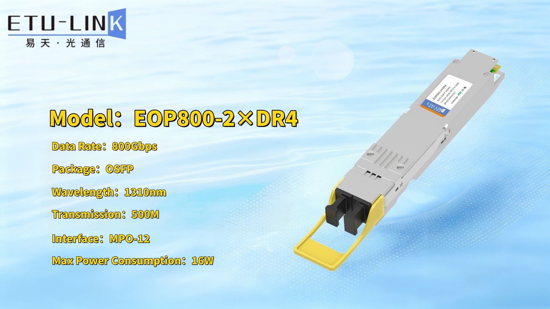
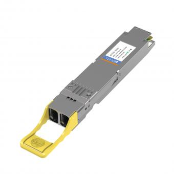
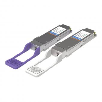
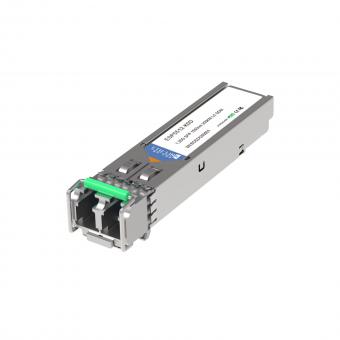
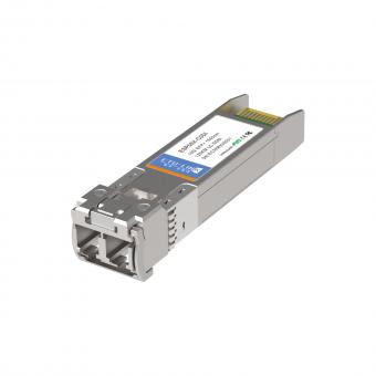
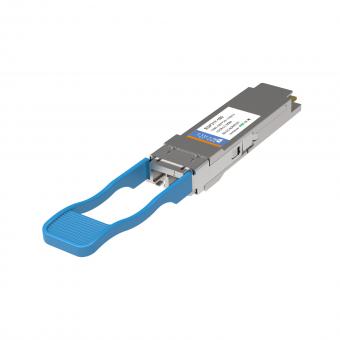
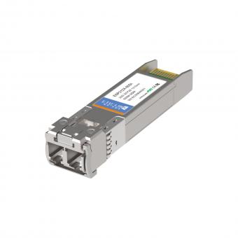
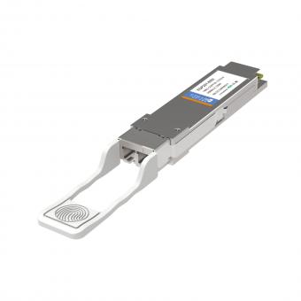
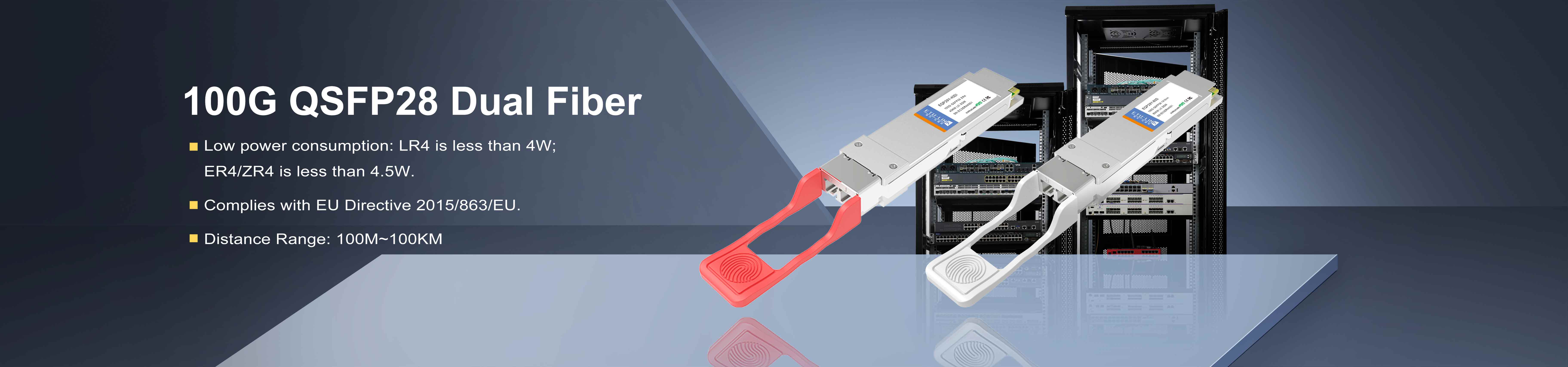
SFP is a single-channel standard with lower data rates and has been gradually replaced by higher-level packages. Currently, the mainstream 400G optical modules mainly use two packages: QSFP-DD and OSFP. QSFP-DD has double the number of channels and better compatibility; OSFP has an eight-channel interface and a larger size. Both place higher demands on PCB wiring density and signal integrity.
The manufacturing process is also under pressure. COB packaging directly mounts the chip onto the PCB surface, resulting in a short signal path and low loss, but it places extremely high demands on board flatness and fine wiring. Packaging upgrades are simultaneously driving material upgrades, with RCC material becoming the core direction for next-generation optical module PCB due to its ability to more stably achieve fine lines of ≤10μm.
From SFP to QSFP and OSFP, the more compact the package and the higher the speed, the more precise the PCB must be—with finer linewidths and more expensive materials. This is the complete chain of AI driving PCB upgrades.
Conclusion
For inquiries about our products or pricelist, please leave your information with us and we will be in touch with in 24 hours.


 13th Floor, Building 6, Honghualing Base, Nanshan Intelligent Manufacturing Base, Liuxian Avenue, Taoyuan Street, Xili, Nanshan District, Shenzhen, China
© Copyright: 2026 ETU-Link Technology CO ., LTD All Rights Reserved.

IPv6 network supported
Friendly Links:
易天官网