English



Part I: The Relationship Between PCB and AI
When people mention PCB (Printed Circuit Board), many think of it as just an ordinary green board used in electronic products for soldering chips and connecting cables. But few know that in today's era of skyrocketing AI computing power, a dedicated PCB for AI servers costs 1000 times more than a circuit board for ordinary household appliances!
Today we'll break down the seemingly insignificant PCB and see how it has caught the AI wave and achieved an epic leap in value.
PCB stands for Printed Circuit Board. Its core function is singular: to connect hundreds of scattered electronic components such as chips, resistors, and capacitors into a unified whole, undertaking three irreplaceable functions within a device:
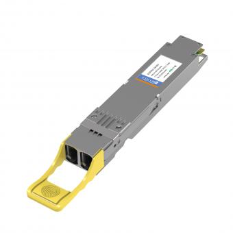
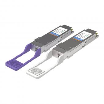
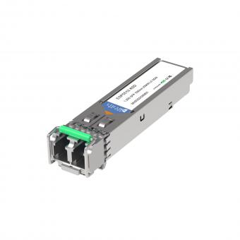
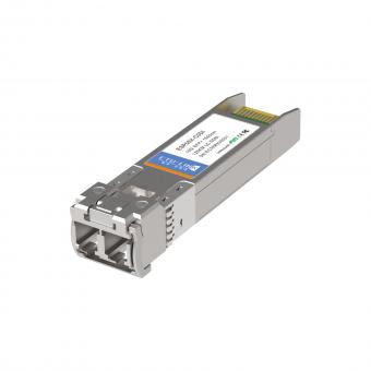
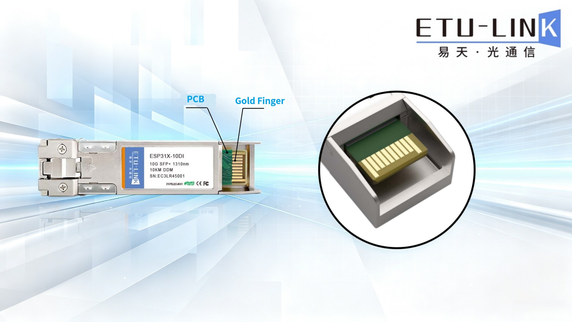
Internal DSP chip, TOSA/ROSA optical transmitter/receiver components, driver/transimpedance amplifiers, capacitors, resistors, and gold finger interfaces of the optical module are all soldered and fixed on the PCB. It also matches SFP/ QSFP/ QSFP-DD/ OSFP package sizes, constraining the overall structure and enabling standardized plug-and-play connections to switches and servers. This serves as the sole mounting substrate for all components of the optical module.
2. The Core Nerves for High-Speed Signal Transmission (Most Critical Value)
The internal copper wires carry electrical signals and transmit power, serving as a high-speed channel for data exchange. High-end AI boards can achieve signal rates of over 56Gbps.
3. Efficient Heat Dissipation: Solving the High Power Consumption Challenge of High-Speed Optical Modules
The biggest pain point of 800G, 1.6T high-speed optical modules is high heat generation and high power consumption .
The thick copper structure and large-area thermal conductive layer of the PCB form the core heat dissipation path of the whole machine, which can quickly conduct the heat of the chip and optical device to the module shell, avoid high temperature sluggishness and high temperature failure, and greatly improve the reliability and service life of the product.
II. The AI Wave Sweeps Through the Entire Supply Chain, Leading a Sharp Rise in PCB Value
Explosive Growth in Computing Power Demand: Global demand for computing power to train large AI models has surged nearly 100 times in 3 years, and the computing power gap continues to widen;
Surge in GPU Shipments: a certain company upgraded its H100 to the B200, and another upgraded its 910B to the 910C. Global AI GPU shipments are expected to reach approximately 5 million units in 2024, representing a year-on-year increase of over 50%.
Large-Scale Expansion of AI Server Production: each model is equipped with 8 to 16 GPUs, and global AI server shipments reached approximately 1.65 million units in 2024, a year-on-year increase of 40%.
Leap in PCB Unit Prices: the price of a regular server motherboard PCB is about $500, while the price of a dedicated AI server motherboard is $3,000 to $5,000, a six-fold increase in value per unit, marking the formal restructuring of the PCB industry's value.
Industry data shows that the global AI server PCB market size reached US$8-10 billion in 2024, accounting for about 12% of the total global PCB market size. It has become the golden segment with the strongest growth certainty and the highest profit margin in the entire PCB industry.
III. PCB Layering: The More Layers and the Narrower the Trace Width, the Higher the Value
| PCB Category | Specifications | Market Unit Price | Core Applications | Industry Gross Margin |
| Single-sided PCB | 1-layer base structure | $0.3 to $2 | Low-end consumer electronics such as remote controls and toys | Low |
| Double-sided PCB | 2-layer trace structure | $2-$10 | Home appliances, general industrial control equipment | Slightly Low |
| Standard multilayer PCB | 4–20-layer laminated structure | $10 to $200 | Traditional servers, automotive electronics, and communication equipment | Moderate |
| HDI (High-Density Interconnect) PCB | Trace width: 50–100 μm; precision blind/buried via technology | $50 to $500 | High-speed boards for AI servers and motherboards for flagship smartphones | 25%–30% |
| FPC (Flexible Printed Circuit) | Flexible polyimide substrate; bendable and rollable | $5-$50 | Foldable smartphones and smart wearable devices | 20%–25% |
| IC Packaging Substrate | Trace width: <20 μm; suitable for chip-level packaging | $100 to $2000 | Underlying packaging of high-end chips such as GPU and CPU | 30%–40% |
In short, the more layers, the finer the linewidth, and the higher the technological barriers, the greater the profit margin for PCB. AI computing power demands are concentrated in three high-margin sectors: HDI high-speed boards, high-end multilayer boards, and packaging substrates. 800G and above OSFP / QSFP-DD optical modules, coherent ZR optical modules , and next-generation CPO co-packaged optical engines all require HDI precision PCB and high-end packaging substrates.
IV. Technological Barriers: Triple Core Processes Build a Moat for the High-End PCB Industry
1.Multi-layer precision lamination barriers. Ordinary PCB have only 4-12 layers, while AI server PCB are upgraded to 20-32 layers. The interlayer spacing is extremely small, the alignment accuracy is at the micrometer level, the process error tolerance is extremely low, and even a slight deviation will cause the entire board to be scrapped, which requires extremely high production control capabilities.
2.High-frequency, low-loss material barriers. High-speed AI computing scenarios need to support signal transmission of 56Gbps or more, which requires the use of high-end low-loss resins and high-frequency special substrates to reduce signal attenuation and interference. These core materials have high technological barriers and are difficult to produce domestically.
3. Ultra-fine circuit process barriers. The line width of high-end AI PCB has been compressed from 100μm to less than 50μm, which requires the use of high-precision SAP/mSAP processes to adapt to advanced GPU packaging. The yield control is difficult, and it is difficult for small and medium-sized manufacturers to achieve mass production breakthroughs.
With three layers of technological barriers filtering out competitors, only leading manufacturers that have mastered the complete set of core processes can enter the leading computing power supply chain and continue to enjoy the long-term benefits of AI computing power expansion.
In Conclusion
In the past, PCB were little-known traditional electronic components, surviving through fierce competition based on low-price mass production. Today, high-end PCB have become the core infrastructure for the AI computing power race. The essence of computing power competition is hardware competition, and PCB, as the underlying foundation supporting the operation of all AI computing power, have completely rewritten the industry's value logic and ushered in a new period of high prosperity and growth due to their extremely high technological barriers and essential nature.
Preview of the Next Issue
In this article, we dissected the value logic , market growth , product segmentation, and technological barriers of PCB in the AI era. In the next installment, we will delve deeper into the core aspects, focusing on the key material systems in PCB manufacturing and the essential upgrade requirements of PCB in AI computing scenarios. We will unlock the layers of truth behind the high premiums of PCB, bringing a more detailed and practical industry analysis. Stay tuned!
Categories
New Blog
Tags
For inquiries about our products or pricelist, please leave your information with us and we will be in touch with in 24 hours.


 13th Floor, Building 6, Honghualing Base, Nanshan Intelligent Manufacturing Base, Liuxian Avenue, Taoyuan Street, Xili, Nanshan District, Shenzhen, China
© Copyright: 2026 ETU-Link Technology CO ., LTD All Rights Reserved.

IPv6 network supported
Friendly Links:
易天官网